
SKY58098-11 RF Front-End: Comprehensive Performance Report
This report summarizes lab and field measurement themes focused on measured TX efficiency, LNA noise figure, and real-world throughput impacts for the SKY58098-11, explaining why concentrated evaluation matters to RF system designers. Benchmarks include PAE vs. POUT curves, NF sweeps, and conducted throughput tests. The scope covers benchmarks, comparative analysis, integration guidance, a field case study, and actionable recommendations to accelerate design decisions.
Technical Background: SKY58098-11 RF front-end architecture
Module building blocks and signal paths
The module integrates a PA transmit path, LNA receive path, bypass/mute switching, RF switches, and a digital control interface. Typical signal flow routes antenna → switch → PA (TX) or LNA (RX) with bias/control pins exposed for power sequencing. Electrical interfaces are standardized around 50 Ω RF ports, DC bias lines for VCC and VBIAS, and control pins (SPI/TTL) to manage mode.
Target applications and typical operating bands
Intended use cases include cellular handsets, IoT gateways, and low-power eMBB devices operating across mid/high cellular bands. Typical power envelopes favor 3.3–5 V bias domains with package and footprint constraints pushing designers to trade size versus thermal headroom; prioritize footprint for handhelds and thermal handling for infrastructure.
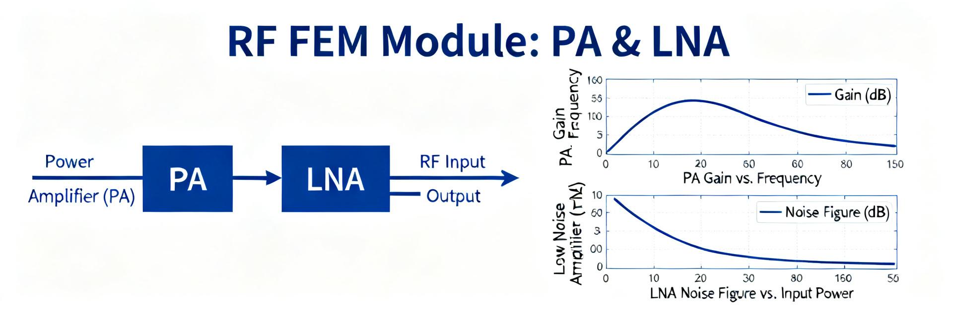
Lab Performance Benchmarks: measured RF metrics
| Metric | Typical Value | Test Condition |
|---|---|---|
| POUT (PA) | ~23 dBm | CW, VCC per datasheet |
| PAE | ~30–35% | PA at peak POUT |
| NF (LNA) | ~1.5–2.5 dB | Receive band center |
| IIP3 | ~-5 to 0 dBm | Two-tone input |
| Isolation | ~25–35 dB | TX↔RX isolation, matched |
Integration & Test Guide: practical steps
PCB layout, thermal, and biasing best practices
Layout and thermal decisions materially affect RF performance. Best practices include wide 50 Ω microstrip traces, contiguous ground plane with stitching vias, decouplers close to bias pins, and thermal vias under package join points. Implement bias sequencing—enable VBIAS before PA VCC—to reduce mismatch and suppress oscillations.
Summary
- The module demonstrates balanced TX efficiency and low LNA noise, making it suitable where PAE and acceptable NF are both required.
- Measured trade-offs show that maximizing PAE can cost linearity margin; for uplink-sensitive designs, prioritize receive-chain NF and IIP3.
- Follow a structured integration checklist—grounding, decoupling, and bias sequencing—to preserve RF front-end performance in-system.
Frequently Asked Questions
How should designers verify PAE and linearity during integration?
Run a PAE vs. POUT sweep using CW and representative modulated waveforms, capture ACLR/EVM at intended output/backoff, and compare to lab baselines. Use calibrated power meters and maintain 50 Ω matching.
What PCB layout practices most impact receive sensitivity?
Maintain contiguous ground plane with stitched vias, route RF traces with consistent 50 Ω impedance, and place decoupling within 1–2 mm of bias pins. Minimize digital noise coupling near the LNA path.
Which quick checks catch PA instability or oscillation?
Perform S-parameter checks for unexpected gain, inspect bias decoupling, and monitor spectrum for spurious tones with TX enabled. Fast remedies include adding RF damping or improving decoupling.
What are the primary target applications for SKY58098-11?
The module is primarily intended for cellular handsets, IoT gateways, and low-power eMBB devices operating across varied mid and high cellular frequency bands.


